


This article describes RF converter design, along with block diagrams, describing RF upconverter design and RF downconverter design. It mentions the frequency components used in this C-band frequency converter. The design is carried out on a microstrip board using discrete RF components such as RF mixers, local oscillators, MMICs, synthesizers, OCXO reference oscillators, attenuator pads, etc.
RF up converter design
RF frequency converter refers to conversion of frequency from one value to the other. The device which converts frequency from low value to high value is known as up converter. As it works at radio frequencies it is known as RF up converter. This RF Up converter module translates IF frequency in the range of about 52 to 88 MHz to RF frequency of about 5925 to 6425 GHz. Hence it is known as C-band up converter. It is used as one part of RF transceiver deployed in the VSAT used for satellite communication applications.
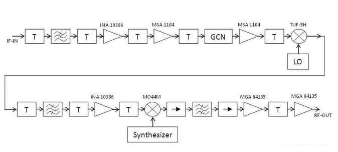
Figure-1 : RF up converter block diagram
Let us see design of RF Up converter part with step by step guide.
Step 1: Find out Mixers, Local oscillator, MMICs, synthesizer, OCXO reference oscillator, attenuator pads generally available.
Step 2: Do the power level calculation at various stages of the lineup especially at the input of MMICs such that it will not exceed 1dB compression point of the device.
Step 3: Design and proper Micro strip based filters at various stages to filter out unwanted frequencies after mixers in the design based on which part of frequency range you want to pass.
Step 4: Do the simulation using microwave office or agilent HP EEsof with proper conductor widths as required at various places on the PCB for chosen dielectric as required for RF carrier frequency. Do not forget to use shielding material as enclosure during simulation. Check for S parameters.
Step 5: Get the PCB fabricated and solder the purchased components and solder the same.
As depicted in the block diagram of figure-1, appropriate attenuator pads of either 3 dB or 6dB need to be used in between to take care of 1dB compression point of the devices (MMICs and Mixers).
Local oscillator and Synthesizer of appropriate frequencies need to be used based. For 70MHz to C band conversion, LO of 1112.5 MHz and Synthesizer of 4680-5375MHz frequency range is recommended. The rule of thumb for choosing mixer is the LO power should be 10 dB greater than the highest input signal level at P1dB. GCN is Gain Control Network designed using PIN diode attenuators which vary attenuation based on analog voltage. Remember to use Band Pass and Low pass filters as and when required to filter out unwanted frequencies and pass the wanted frequencies.
RF Down converter design
The device which converts frequency from high value to low value is known as down converter. As it works at radio frequencies it is known as RF down converter. Let us see design of RF down converter part with step by step guide. This RF down converter module translates RF frequency in the range from 3700 to 4200 MHz to IF frequency in the range from 52 to 88 MHz. Hence it is known as C-band down converter.
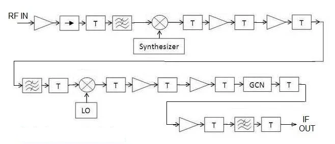
Figure-2 : RF down converter block diagram
The figure-2 depicts block diagram of C band down converter using RF components. Let us see design of RF down converter part with step by step guide.
Step 1: Two RF mixers have been selected as per Heterodyne design which converts RF frequency from 4 GHz to 1GHz range and from 1 GHz to 70 MHz range. The RF mixer used in the design is MC24M and IF mixer is TUF-5H.
Step 2: Appropriate filters have been designed to be used at different stages of the RF down converter. This include 3700 to 4200 MHz BPF, 1042.5 +/- 18 MHz BPF and 52 to 88 MHz LPF.
Step 3:MMIC amplifier ICs and attenuation pads are used at appripriate places as shown in the block diagram to meet power levels at the output and input of the devices. These are choosen as per gain and 1 dB compression point requirement of the RF down converter.
Step 4: RF synthesizer and LO used in the up converter design are also used in the down converter design as shown.
Step 5: RF isolators are used at appropriate places to allow RF signal to pass in one direction (i.e. forward) and to stop its RF reflection in the backward direction. Hence it is known as uni-directional device. GCN stands for Gain control network. The GCN functions as variable attenuation device which allows setting of RF output as desired by RF link budget.
Conclusion: Similar to the concepts mentioned in this RF frequency converter design, one can design frequency converters at other frequencies such as L band, Ku band and mmwave band.
Post time: Dec-07-2023


