


In microwave circuits or systems, the entire circuit or system is often composed of many basic microwave devices such as filters, couplers, power dividers, etc. It is hoped that through these devices, it is possible to efficiently transmit signal power from one point to another with minimal loss;
In the entire vehicle radar system, energy conversion mainly involves the transfer of energy from the chip to the feeder on the PCB board, the transfer of the feeder to the antenna body, and the efficient radiation of energy by the antenna. In the entire energy transfer process, an important part is the design of the converter. The converters in millimeter wave systems mainly include microstrip to substrate integrated waveguide (SIW) conversion, microstrip to waveguide conversion, SIW to waveguide conversion, coaxial to waveguide conversion, waveguide to waveguide conversion and different types of waveguide conversion. This issue will focus on microband SIW conversion design.
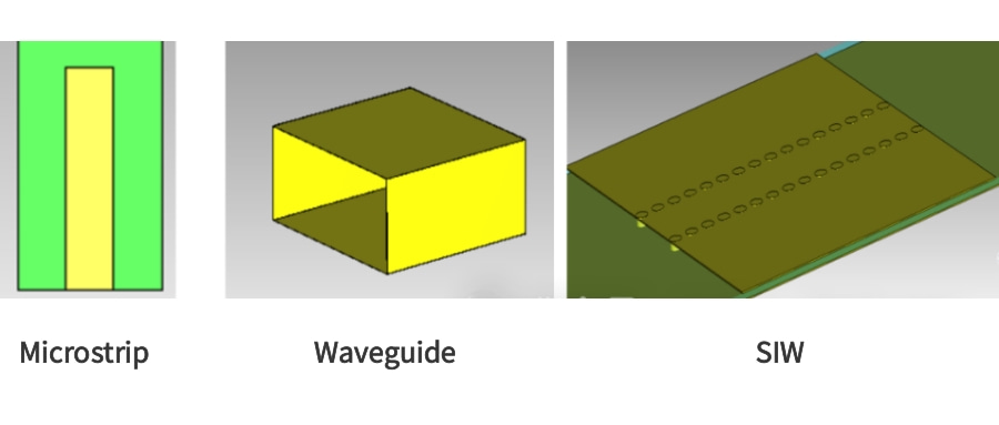
Different types of transport structures
Microstrip is one of the most widely used guide structures at relatively low microwave frequencies. Its main advantages are simple structure, low cost and high integration with surface mount components. A typical microstrip line is formed using conductors on one side of a dielectric layer substrate, forming a single ground plane on the other side, with air above it. The top conductor is basically a conductive material (usually copper) shaped into a narrow wire. Line width, thickness, relative permittivity, and dielectric loss tangent of the substrate are important parameters. Additionally, the thickness of the conductor (i.e., metallization thickness) and the conductivity of the conductor are also critical at higher frequencies. By carefully considering these parameters and using microstrip lines as the basic unit for other devices, many printed microwave devices and components can be designed, such as filters, couplers, power dividers/combiners, mixers, etc. However as frequency increases (when moving to relatively high microwave frequencies) transmission losses increase and radiation occurs. Therefore, hollow tube waveguides such as rectangular waveguides are preferred because of smaller losses at higher frequencies (no radiation). The interior of the waveguide is usually air. But if desired, it can be filled with dielectric material, giving it a smaller cross-section than a gas-filled waveguide. However, hollow tube waveguides are often bulky, can be heavy especially at lower frequencies, require higher manufacturing requirements and are costly, and cannot be integrated with planar printed structures.
RFMISO MICROSTRIP ANTENNA PRODUCTS:
RM-MA25527-22,25.5-27GHz
RM-MA425435-22,4.25-4.35GHz
The other is a hybrid guidance structure between a microstrip structure and a waveguide, called a substrate integrated waveguide (SIW). An SIW is an integrated waveguide-like structure fabricated on a dielectric material, with conductors on top and bottom and a linear array of two metal vias forming the sidewalls. Compared with microstrip and waveguide structures, SIW is cost-effective, has a relatively easy manufacturing process, and can be integrated with planar devices. In addition, the performance at high frequencies is better than that of microstrip structures and has waveguide dispersion properties. As shown in Figure 1;
SIW design guidelines
Substrate integrated waveguides (SIWs) are integrated waveguide-like structures fabricated by using two rows of metal vias embedded in a dielectric connecting two parallel metal plates. Rows of metal through holes form the side walls. This structure has the characteristics of microstrip lines and waveguides. The manufacturing process is also similar to other printed flat structures. A typical SIW geometry is shown in Figure 2.1, where its width (i.e. the separation between vias in the lateral direction (as)), the diameter of the vias (d) and the pitch length (p) are used to design the SIW structure The most important geometric parameters (shown in Figure 2.1) will be explained in the next section. Note that the dominant mode is TE10, just like the rectangular waveguide. The relationship between the cutoff frequency fc of air-filled waveguides (AFWG) and dielectric-filled waveguides (DFWG) and dimensions a and b is the first point of SIW design. For air-filled waveguides, the cutoff frequency is as shown in the formula below
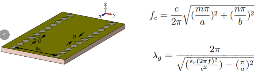
SIW basic structure and calculation formula[1]
where c is the speed of light in free space, m and n are the modes, a is the longer waveguide size, and b is the shorter waveguide size. When the waveguide works in TE10 mode, it can be simplified to fc=c/2a; when the waveguide is filled with dielectric, the broadside length a is calculated by ad=a/Sqrt(εr), where εr is the dielectric constant of the medium; in order To make SIW work in TE10 mode, the through hole spacing p, diameter d and wide side as should satisfy the formula on the upper right of the figure below, and there are also empirical formulas of d<λg and p<2d [2];
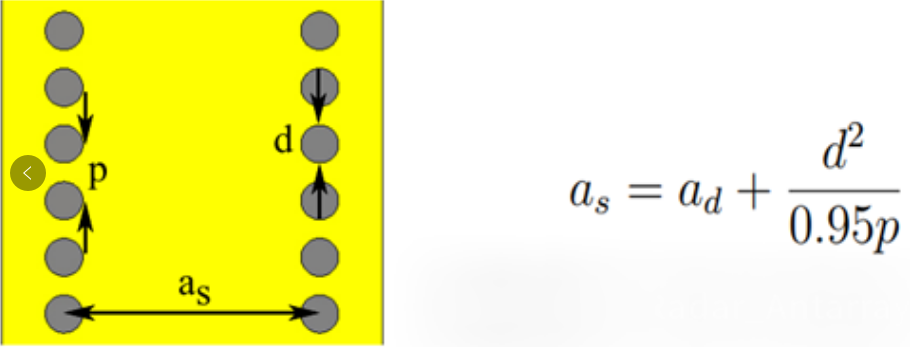
where λg is the guided wave wavelength: At the same time, the thickness of the substrate will not affect the SIW size design, but it will affect the loss of the structure, so the low-loss advantages of high-thickness substrates should be considered.
Microstrip to SIW conversion
When a microstrip structure needs to be connected to a SIW, the tapered microstrip transition is one of the main preferred transition methods, and the tapered transition usually provides a broadband match compared to other printed transitions. A well-designed transition structure has very low reflections, and insertion loss is primarily caused by dielectric and conductor losses. The selection of substrate and conductor materials mainly determines the loss of the transition. Since the thickness of the substrate hinders the width of the microstrip line, the parameters of the tapered transition should be adjusted when the thickness of the substrate changes. Another type of grounded coplanar waveguide (GCPW) is also a widely used transmission line structure in high-frequency systems. The side conductors close to the intermediate transmission line also serve as ground. By adjusting the width of the main feeder and the gap to the side ground, the required characteristic impedance can be obtained.
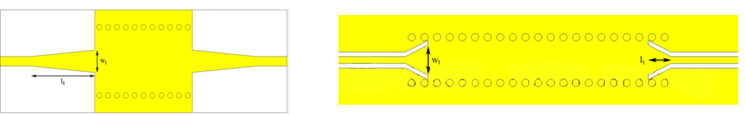
Microstrip to SIW and GCPW to SIW
The figure below is an example of the design of microstrip to SIW. The medium used is Rogers3003, the dielectric constant is 3.0, the true loss value is 0.001, and the thickness is 0.127mm. The feeder width at both ends is 0.28mm, which matches the width of the antenna feeder. The through hole diameter is d=0.4mm, and the spacing p=0.6mm. The simulation size is 50mm*12mm*0.127mm. The overall loss in the passband is about 1.5dB (which can be further reduced by optimizing the wide-side spacing).
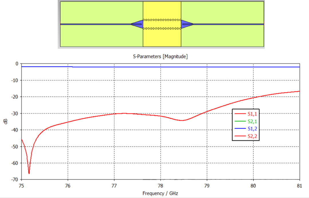
SIW structure and its S parameters
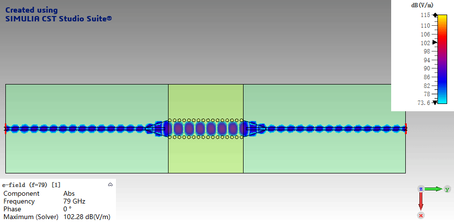
Electric field distribution@79GHz
Post time: Jan-18-2024


